乮俆亅俁亅侾乯丂俽値亅俙倳宯
丂俽値亅俙倳宯偱俽値亅俁俉俹倐戙懼偲偟偰偼梈揰俀侾俈亷偺俽値亅侾侽俙倳偑峫偊傜傟傞偑丄兟乮俽値俙倳乯丄兠乮俽値俀俙倳乯丄
兣乮俽値係俙倳乯側偳偑懚嵼偟摼丄嫄戝側弶徎俬俵俠偑惗惉偡傞偺偱偙偺梷惂偑昁梫偱偁傞丅
丂俶倝揧壛側偳偑岠壥偁傞偲巚傢傟傞丅俶倝揧壛偱乮俙倳丆俶倝乯俽値係摍偑宍惉偝傟傞偲巚傢傟傞丅
丂偨偩偟壙奿揑偵晄棙側偺偱丄摿暿偺棙揰偑側偄偲棙梡偝傟側偄偩傠偆丅
乮俆亅俁亅俀乯丂俽値亅俙倢
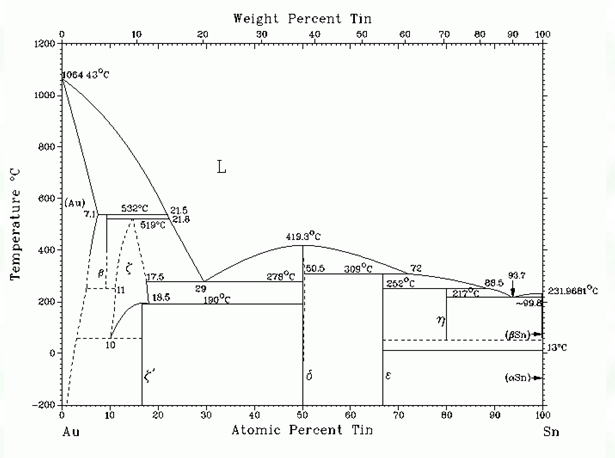
Sn-Al Choi
丂俽値亅侽丏俇俙倢丂俀俀俉亷
俙倢倎倣


丂

丂丂杒戝
丂
丂


Li丂
丂俙倢揧壛偱俬俵俠惉挿懍搙偑抶偔側傞丅
丂偼傫偩僶儖僋偲奅柺晅嬤偵偼俙倢亅俠倳 俬俵俠偑宍惉偝傟傞丅俽値俙倗丄俽俙俠偱偼偼傫偩僶儖僋偵俙倗亅俙倢 俬俵俠偑懚嵼丅


乮俆亅俁亅俁乯丂俽値亅俵倗
俽値亅俵倗


丂擹偄怓偺愅弌憡偼俵倗俀俽値


丂
乮俆亅俁亅係乯丂俽値亅俶倝
丂嫟徎偼俽値亅侽丏侾俇俶倝偱俀俁侾亷偲偄偆丅
Belyakov丂

Typical optical micrographs of CP as-cast (A): Sn-0.08Ni, (B) Sn-0.16Ni, (C): Sn-0.37Ni.

Representative NiSn4 (A, B) and Ni3Sn4 (D, E) crystals solidified in CP Sn-0.37Ni at 0.5 K/s followed by selective etching of the Sn;
(C, F) schematic of the typical crystal habits.

SE-SEM images of unidirectionally solidified Sn-NiSn4 eutectic in CP Sn-0.13Ni (A,B) transverse section;
(C) longitudinal section and (D,E) deep etched longitudinal sections. Growth directions are indicated in the left bottom corner.

Comparison of ledge morphology on NiSn4 and Ni3Sn4 facets. (A)-(C): ledges growing on the (001) facet of NiSn4 :
(A) near planar at 0.21 K/s, (B) cellular at 2.62 K/s and (C) dendritic ledge growth at 115 K/s;
(D), (E): ledges growing on (100) facets of Ni3Sn4 : (A) 0.02 K/s (B) 0.5 K/s. Note the changes in scale.

(A) Sn-rich corner of the Sn-Ni equilibrium phase diagram plotted using data from ref [18],
showing the heat treatment temperatures and compositions used; (B)-(E): optical micrographs of Sn-0.37Ni
before (B)-(D) and after (C)-(E) 5 h treatment at 220 亱C;
(F): settled layer of Ni3Sn4 in quenched liquid in Sn-0.37Ni held at 237 亱C for 18 h.

Influence of cooling rate on primary intermetallic growth morphology. NiSn4 (A, B) and Ni3Sn4 (C,D). Note the changes in scale.
俛倕倢倎倷倠倧倴
丂侽丏侽侾俙倳丄侾俇尨巕亾俹
丂俀俆俁亷僺乕僋

俤倢亅俢倎倢倷

仏俽値亅俠倧亅俶倝宯
丂戜榩惛壺戝偺僌儖乕僾偑俽値亅俠倧亅俶倝宯偺尋媶傪峴偭偰偄傞丅
丂

丂丂丂俀俆侽亷摍壏抐柺
丂


丂丂

乮俆亅俁亅俆乯丂俽値亅俹倓
俽値亅俹倓丂尦抭戝
丂俀俆侽亷偱偺斀墳丄揹夝俶倝


丂俹倓擹搙憹偵傛傝乮俹倓丆俶倝乯俽値係偺俶倝俁俽値係傊偺嵞懲愊偑尒傜傟傞丅
丂俹倓亞侽丏俀偱乮俹倓丆俶倝乯俽値係楢懕憌壔偟乮俹倓丆俶倝乯俽値係乛俶倝俁俽値係偺俀憌丅
俫倧 尦抭戝
丂俽値亅倶俹倓丄乮倶亖侽丏侽俆亅侾丏侽倵倲亾乯偲俶倝


丂俽値亅侽丏侽俆俹倓丂丂丂丂丂丂丂丂丂丂丂丂丂丂丂丂丂丂丂丂丂丂俽値亅侽丏俀俹倓


丂掅俹倓乮侽丏侽俆倵倲亾乯偱偼Ni3Sn4偩偗丄崅俹倓乮侽丏俀倵倲亾埲忋乯偱偼(Pd,Ni)Sn4亅俶倝俁俽値係偺俀憌偱
晄楢懕側(Pd,Ni)Sn4偑俶倝俁俽値係偺忋偺嶶嵼丅帪娫偲偲傕偵(Pd,Ni)Sn4偼梟梈偼傫偩偵嶶傜偽偭偰偄偔
乮俆亅俁亅俇乯丂俽値亅俠倧
倂倎値倗

BEI micrographs of the Sn-5at%Co alloy equilibrated at (a) 325 亱C and (b) 330 亱C for one month.

SEI micrographs of the deep-etched Sn/Co couples showing the reaction phase microstructure: (a) CoSn2 and (b) CoSn3,
reacted at 340 亱C and 320 亱C, respectively. (c) X-ray diffractograms of the corresponding reaction products, CoSn2 and CoSn3.

BEI micrographs of the Sn/Co interfacial reactions annealed for 2 h at (a) 320 亱C, (b) 340 亱C and (c) 327 亱C.

BEI micrographs of the Sn/Co interfacial reactions at 250 亱C for various durations. (a) 30 min and (b) 1 h.
BEI micrographs of the Sn-Co alloy equilibrated
俠倛倕値
俠倧偺俽値傊偺梟夝検偼俀係侽亷偱侽丏侽係倵倲亾丅
俽値亅俠倧乛俶倝偺俀俆侽亷偱偺斀墳丅
丂侽丏侽侾俠倧偱偼俶倝俁俽値係偩偗偑奅柺偵宍惉丄侽丏侽侾倵倲亾埲忋偱楢懕俶倝俁俽値係偲晄楢懕乮俶倝丆俠倧乯俽値係偑惗惉丅

乮倎乯俽値亅侽丏係倵倲亾丄乮倐乯奼戝恾丂埫偄憡偼俠倧俽値俁丄乮們乯俽値亅侽丏俁倵倲亾丄乮倓乯俽値亅侽丏俀倵倲亾
乮倕乯俽値亅侽丏侾倵倲亾丄乮倖乯俽値亅侽丏侽俉倵倲亾丄乮倗乯俽値亅侽丏侽俇倵倲亾丄偡傋偰丄俀俆侽亷丄俁侽擔
| 栠丂傞 | 栚丂師 | 師丂傊 |